

UHF6S – Pure Silicon Technology
HIGH-SPEED TECHNOLOGY FOR INDUSTRIAL
AND CONSUMER APPLICATIONS
To get easy access to our foundry, customers can either participate in a Multi-Project Wafer at a fixed cost or order a fully dedicated technology run (Engineering Run) to their request.
Applications
• Tailored for Frequencies from DC up to 2.4 GHz
• Cellular Systems
• Networking Systems
• Wireless Systems (e.g., WLAN, DECT, RF Control)
• Laser Drivers
• High-speed Operational Amplifiers
• Photo-detecting Devices
Features
• Complementary NPN and VPNP
• Low Parasitic Capacitances
(e.g., Minimum Collector Substrate Capacitance is 12 fF)
• Very Low Leakage Levels
• Photo Diode Available
Multi Project Wafer Runs (MPW)
• Every 90 Days
Design Kits
• Cadence®
UHF6S is best suited for wireless communications, RF control, and high-speed digital as well as driver applications up to 2.4 GHz. UHF6S offers all kinds of standard devices plus optional devices not common in competitive technologies.
With its unique features and devices, UHF6S enables superior application and customer-specific solutions such as RF control circuits in the 315 MHz-900 MHz ISM bands with industry-leading edge sleep current of typically less than 1 nA, laser driver circuits for CD/DVD writing applications achieving pulses of 0.8 ns rise time at peak currents of up to 500 mA, and photo detecting devices for CD and DVD applications.
With its unique features and devices, UHF6S enables superior application and customer-specific solutions such as RF control circuits in the 315 MHz-900 MHz ISM bands with industry-leading edge sleep current of typically less than 1 nA, laser driver circuits for CD/DVD writing applications achieving pulses of 0.8 ns rise time at peak currents of up to 500 mA, and photo detecting devices for CD and DVD applications.
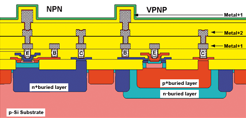
Schematic Cross Section of UHF6S Key Devices
Technical Parameters
NPN-SIC |
NPN |
VPNP |
|
| Minimum emitter area [µm2] | 0.5 x 0.7 |
0.5 x 0.7 |
0.5 x 0.7 |
| Beta | 90 |
70 |
35 |
| BVCBo [V] | 12 |
21 |
16 |
| BVCEo [V] | 3.3 |
6.5 |
7.0 |
| fT [GHz] | 33 |
17 |
12 |
| Resistor values [Ω /sq] | 8/90/2000 |
||
| Double-poly capacitor [fF/µm2] | 3.1 |
||
Photo diode Optimized for wave length [nm] Responsivity [A/W] |
650 and 785 > 0.45 |
||
| Additional devices | Versatile set of further active and passive devices (see Design Kit) |
||
| Minimum contact size [µm2] | 0.8 x 0.8 |
||
| Metal-1 pitch [µm] | 2.0 |
||
| Number and type of metal layers | 3 AlSiCu |
||