
High-voltage BCDMOS/BCD-on-SOI
Technology with 120V Option
BCD-on-SOI combines Bipolar, CMOS and DMOS (= BCDMOS) technology on SOI substrate. This enables simultaneous handling of analog and digital power to realize smart power devices for automotive, telecommunication and consumer electronics.
Applications
• Power Management Systems
• 42 V Automotive Board Network
• Class D Audio Amplifiers
• Smart Motor Control/CD Drivers
• ADSL Line Drivers, POE
• High-temperature Sensors
Benefits
• High-temperature and High-voltage Capability
• Small Size (Gate Density Equivalent to 0.5 μ CMOS)
• Insensitive Against Intrinsic Radiation
• Reduced Rdson due to SOI
• Less Parasitics for Simpler Design
Features
• Fully Dielectric Isolated Twin Well, 3 Metal Layers Operating up to 200°C
• High-density 5 V N- and P-MOS Transistors
• DMOS High-voltage Capability up to 120 V
• DMOS Family for 25, 45, 65 and 80 V as Standard Available
• Additional 120 V Option
• Bipolar PNP and NPN Transistors Available
• Patented DMOS Method for Optimized Trade-off between Vbreakdown and Rdson
Technical Parameters
| Parameters | Value |
| Lithography | 0.8 (0.5*) µm |
| Maximum voltage | 80 V (120 V) |
| Base devices | 5 V CMOS, N/P HVMOS, LPNP, LNPN, Zener, freewheeling and blocking diodes |
| Metallization | 3 level AISiCu |
| Minimum Rdson | 0.06 Ω mm2 |
| Packaging density | 4000 gates/mm2 |
| N-DMOS/N-MOS FT | 3/15 GHz |
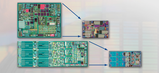
Size Comparison of BCDMOS Bulk Technology and SOI
SOI: die-cost reduction(including Spec. Changes)
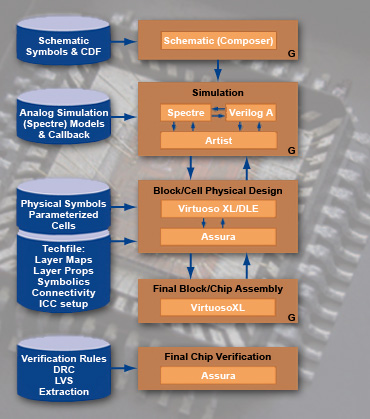
Development Support
Cadence® PDK/Starter Kit• MPW Every 60 Days
• Engineering Runs Available
• DRC and LVS Verification
• Device Models for SPECTRE, HSPICE and ELDO
• SOA Option Involved in PDK
• PDK Offers Different Levels of Simulation Models